- 您现在的位置:买卖IC网 > Sheet目录3753 > ATMEGA169P-16MCHR (Atmel)MCU AVR 16KB FLASH 16MHZ 64-VQFN
PIC16F946
DS41265A-page 156
Preliminary
2005 Microchip Technology Inc.
FIGURE 12-4:
ANALOG INPUT MODEL
12.3
A/D Operation During Sleep
The A/D converter module can operate during Sleep.
This requires the A/D clock source to be set to the
internal oscillator. When the RC clock source is
selected, the A/D waits one instruction before starting
the conversion. This allows the SLEEP instruction to be
executed, thus eliminating much of the switching noise
from the conversion. When the conversion is complete,
the GO/DONE bit is cleared and the result is loaded
into the ADRESH:ADRESL registers. If the A/D
interrupt is enabled, the device awakens from Sleep. If
the GIE bit (INTCON<7>) is set, the program counter is
set to the interrupt vector (0004h). If GIE is clear, the
next instruction is executed. If the A/D interrupt is not
enabled, the A/D module is turned off, although the
ADON bit remains set.
When the A/D clock source is something other than
RC, a SLEEP instruction causes the present conversion
to be aborted, and the A/D module is turned off. The
ADON bit remains set.
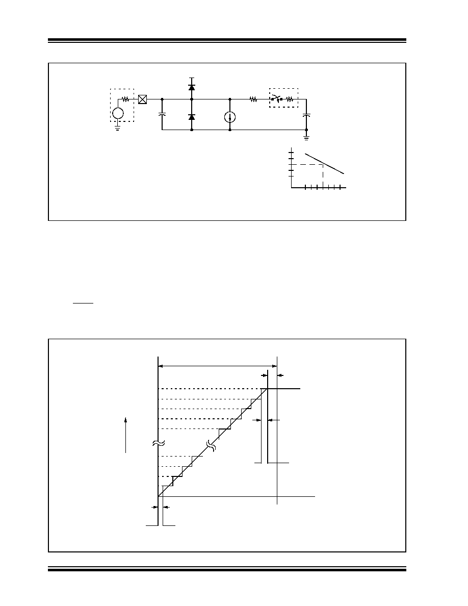
FIGURE 12-5:
A/D TRANSFER FUNCTION
CPIN
VA
RS
ANx
5 pF
VDD
VT = 0.6V
I LEAKAGE
RIC
≤ 1k
Sampling
Switch
SS RSS
CHOLD
= DAC capacitance
VSS
6V
Sampling Switch
5V
4V
3V
2V
567 8 9 10 11
(k
Ω)
VDD
= 10 pF
± 500 nA
Legend: CPIN
VT
I LEAKAGE
RIC
SS
CHOLD
= Input Capacitance
= Threshold Voltage
= Leakage current at the pin due to
= Interconnect Resistance
= Sampling Switch
= Sample/Hold Capacitance (from DAC)
various junctions
RSS
3FFh
3FEh
A/
D
O
u
tpu
t
3FDh
3FCh
004h
003h
002h
001h
000h
Full-Scale
3FBh
1/2 LSB Ideal
Zero-Scale
Transition
V
REF
1/2 LSB Ideal
Transition
Center of
Full-Scale Code
1 LSB Ideal
Full-Scale Range
Analog Input
发布紧急采购,3分钟左右您将得到回复。
相关PDF资料
2-1546217-0
TERM BLK RCPT 20POS SIDE 5.08MM
1-1546217-9
TERM BLK RCPT 19POS SIDE 5.08MM
1-1546217-8
TERM BLK RCPT 18POS SIDE 5.08MM
1-1546217-7
TERM BLK RCPT 17POS SIDE 5.08MM
1-1546217-6
TERM BLK RCPT 16POS SIDE 5.08MM
1-1546217-5
TERM BLK RCPT 15POS SIDE 5.08MM
1-1546217-4
TERM BLK RCPT 14POS SIDE 5.08MM
1-1546217-3
TERM BLK RCPT 13POS SIDE 5.08MM
相关代理商/技术参数
ATMEGA169P-16MCU
功能描述:8位微控制器 -MCU AVR 16KB, 512B EE 16MHz 1KB SRAM, 5V
RoHS:否 制造商:Silicon Labs 核心:8051 处理器系列:C8051F39x 数据总线宽度:8 bit 最大时钟频率:50 MHz 程序存储器大小:16 KB 数据 RAM 大小:1 KB 片上 ADC:Yes 工作电源电压:1.8 V to 3.6 V 工作温度范围:- 40 C to + 105 C 封装 / 箱体:QFN-20 安装风格:SMD/SMT
ATMEGA169P-16MU
功能描述:8位微控制器 -MCU AVR 16K FLASH 512B EE 1K SRAM LCD ADC RoHS:否 制造商:Silicon Labs 核心:8051 处理器系列:C8051F39x 数据总线宽度:8 bit 最大时钟频率:50 MHz 程序存储器大小:16 KB 数据 RAM 大小:1 KB 片上 ADC:Yes 工作电源电压:1.8 V to 3.6 V 工作温度范围:- 40 C to + 105 C 封装 / 箱体:QFN-20 安装风格:SMD/SMT
ATMEGA169P-16MU SL383
制造商:Atmel Corporation 功能描述:MCU 8BIT ATMEGA RISC 16KB FLASH 3.3V/5V 64PIN MLF - Tape and Reel
ATMEGA169P-16MUR
功能描述:8位微控制器 -MCU AVR LCD 16KB FLSH EE 512B 1KB SRAM-16MHZ RoHS:否 制造商:Silicon Labs 核心:8051 处理器系列:C8051F39x 数据总线宽度:8 bit 最大时钟频率:50 MHz 程序存储器大小:16 KB 数据 RAM 大小:1 KB 片上 ADC:Yes 工作电源电压:1.8 V to 3.6 V 工作温度范围:- 40 C to + 105 C 封装 / 箱体:QFN-20 安装风格:SMD/SMT
ATMEGA169P-8AU
制造商:ATMEL 制造商全称:ATMEL Corporation 功能描述:Microcontroller with 16K Bytes In-System Programmable Flash
ATMEGA169P-8MU
制造商:ATMEL 制造商全称:ATMEL Corporation 功能描述:Microcontroller with 16K Bytes In-System Programmable Flash
ATMEGA169PA
制造商:ATMEL 制造商全称:ATMEL Corporation 功能描述:8-bit Microcontroller with 16K Bytes In-System Programmable Flash
ATMEGA169PA_1
制造商:ATMEL 制造商全称:ATMEL Corporation 功能描述:High Endurance Non-volatile Memory segments